SG-8002DC 45.0000M-PCBS 数据手册
Crystal oscillator
Epson Toyocom
Product Number (please contact us)
SG-8002DC: Q3204DCx1xxxx00
SG-8002DB: Q3203DBx1xxxx00
CRYSTAL OSCILLATOR
PROGRAMMABLE
SG - 8002DC / DB series
•Frequency range
•Supply voltage
•Function
:
:
:
1 MHz to 125 MHz
3.3 V / 5.0 V
Output enable(OE) or Standby( ST )
Pin compatible with full size and half size.
•Short mass production lead time by PLL technology.
•SG-Writer available to purchase.
Please contact EPSON TOYOCOM or local sales representative.
Actual size
SG-8002DC
SG-8002DB
Specifications (characteristics)
Item
f0
Output frequency range
Supply voltage
VCC
Storage
temperature
Operating
temperature
Temperature
range
Specifications *2
PT / ST
PH / SH
1 MHz to 125 MHz
4.5 V to 5.5 V
Symbol
-55 °C to +125 °C
T_stg
T_use
-20 °C to +70 °C (-40 °C to +85 °C)
Remarks
PC / SC
VCC=4.5 V to 5.5 V
1 MHz to 125 MHz VCC=3.0 V to 3.6 V
1 MHz to 66.7 MHz VCC=2.7 V to 3.6 V
2.7 V to 3.6 V
Store as bare product after unpacking
-40 °C to +85 °C
Refer to “Outline specifications” (Frequency range)
-20 °C to +70 °C
B: ±50 × 10-6 ,C: ±100 × 10-6
Frequency tolerance
f_tol
M: ±100 × 10-6
-40 °C to +85 °C
*3
Current consumption
Icc
45 mA Max.
28 mA Max.
No load condition, Max. frequency
Disable current
I_dis
30 mA Max.
16 mA Max.
OE=GND(PT,PH,PC)
Stand-by current
I_std
50 μA Max.
ST =GND(ST,SH,SC)
40 % to 60 %
CMOS load:50%Vcc level, Max. load condition
Symmetry *1
SYM
40 % to 60 %
TTL load: 1.4 V level, Max. load condition
High output voltage
VOH
VCC-0.4 V Min.
IOH=-16 mA(PT,ST,PH,SH),-8 mA(PC,SC)
Low output voltage
VOL
0.4 V Max.
IOL=16 mA(PT,ST,PH,SH), 8 mA(PC,SC)
Output load condition (TTL) *1
L_TTL
5 TTL Max.
Max. frequency and
Max. supply voltage
Output load condition (CMOS) *1 L_CMOS
15 pF Max.
25 pF Max.
15 pF Max.
VIH
2.0 V Min.
70 % VCC Min.
Output enable /
ST terminal or OE terminal
disable input voltage
VIL
0.8 V Max.
20 % VCC Max.
3 ns Max.
CMOS load: 20 % VCC to 80 % VCC level
Rise time / Fall time *1
tr / tf
4 ns Max.
TTL load: 0.4 V to 2.4 V level
10 ms Max.
Time at minimum supply voltage to be 0 s
Start-up time
t_str
-6
±5 × 10 / year Max.
+25 °C, VCC=5.0 V/ 3.3 V (PC/SC) First year
Frequency aging
f_aging
*1 Operating temperature (-40 °C to +85 °C), the available frequency, symmetry and output load conditions, please refer to “Outline specifications” page.
*2 PLL-PLL connection & Jitter specification, please refer to “Jitter specifications and characteristics chart” page.
*3 PT / ST and PH / SH for “M” tolerance will be available up to 55 MHz.
Checking possible by the Frequency Checking Program.
External dimensions
(Unit:mm)
SG-8002DC
SG-8002DB
16.0000 C 2PH
EPSON 9357B
13.7 Max. #4
0.2Min.
0.51
7.62
#1
19.8 Max.
#7
7.62
0.25
90°~105°
0.2 Min.
0.51
15.24
Note.
OE Pin (PT, PH, PC)
OE pin = "H" or "open" : Specified frequency output.
OE pin = "L" : Output is high impedance.
Pin map
Pin
Connection
1
OE or ST
7
GND
8
OUT
14
VCC
5.3 Max.
#1
#8
6.36
EPSON
100.0000 C
2PH 9357B
#14
Pin map
Pin
Connection
1
OE or ST
4
GND
5
OUT
8
VCC
2.54 Min.
#5
6.6
#8
2.54 Min. 5.3 Max.
.
7.62
0.25
90°~105°
ST pin (ST, SH, SC)
ST pin = "H" or "open" : Specified frequency output.
ST pin = "L" : Output is low level (weak pull - down), oscillation stops.
To maintain stable operation, provide by-pass capacitor with more than 0.1 μF at a location as near as possible to the power source terminal of the crystal
products (between VCC - GND).
http://www.epsontoyocom.co.jp
�
SG-8002DC 45.0000M-PCBS 价格&库存
很抱歉,暂时无法提供与“SG-8002DC 45.0000M-PCBS”相匹配的价格&库存,您可以联系我们找货
免费人工找货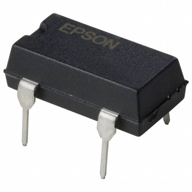


 工商网监
湘ICP备2023018690号
工商网监
湘ICP备2023018690号